 EL
EL EN
EN


- PC Hardware
- Wi-Fi Equipment
- Alarm Systems
- CCTV
- Satellite systems
- Terrestrial systems
- Instruments
- Plastic optical fibers
- Structured Cabling
- Telephonic
- Cabines - Racks
- Industrial Automation
- Solar panels
- FAN,Cooling Systems
- Relay
- Relay 3V
- Relay 5V
- Relay 6V
- Relay 9V
- Relay 12V
- Relay 24V
- relay 48V
- Relay 110V
- Relay 220V
- Automotive Relay
- Industrial Relay Bulb Type Base
- Relay 12VDC bulb type 8p
- Relay 12VDC bulb type 11p
- Relay 12VAC bulb type 8p
- Relay 12VAC bulb type 11p
- Relay 24VDC bulb type 8p
- Relay 24VDC bulb type 11p
- Relay 24VAC bulb type 8p
- Relay 24VAC bulb type 11p
- Relay 48VDC bulb type 8p
- Relay 48VDC bulb type 11p
- Relay 48VAC bulb type 8p
- Relay 48VAC bulb type 11p
- Relay 60VDC bulb type 8p
- Relay 60VDC bulb type 11p
- Relay 110-120VDC bulb type 8p
- Relay 110-120VDC bulb type 11p
- Relay 110-120VAC bulb type 8p
- Relay 110-120VAC bulb type 11p
- Relay 220-230VAC bulb type 8p
- Relay 220-230VAC bulb type 11p
- Relay Impulse step
- Relay on Board
- WiFi Relay
- Various Relay
- Electronic assemblies
- Electronic equipment
- Service parts
- IC
- Optocoupler
- 24LC series
- 4N series
- 5L series
- 74 series
- 78 series
- AD series
- ATT series
- CA series
- CNY series
- DS series
- F series
- H series
- ICL/ISL series
- I series
- K series
- L series
- LM series
- MAX series
- M series
- MOC series
- N series
- NJM series
- OPA series
- PC series
- PLS series
- R series
- SG series
- S series
- STK series
- STRF series
- TC series
- TDA series
- TEA series
- TL series
- TM series
- TN series
- UCxx series
- ULxx series
- V series
- Viper series
- Z series
- Logic series
- IC sockets
- TRN-MOSFET-IGBT
- IGBT-Module
- 2N series
- 2SA series
- 2SB series
- 2SC series
- 2SD series
- 2SK series
- 2SJ series
- 3N series
- 60N series
- 6NK series
- 7824 series
- 7NK series
- A series
- BC series
- BD series
- BF series
- BS series
- BU series
- BUH series
- BUZ series
- F series
- IG series
- Η series
- I series
- IP series
- IR series
- IX series
- J series
- MJ series
- N60 series
- S series
- SUD series
- T11 series
- TCM series
- TI series
- TOP series
- TS series
- ZTX series
- Accessories
- Transformers
- Relay sockets
- Switches
- Terminal blocks
- Pins
- Pins set
- Hole pin with insulation
- Spade pin with insulation
- Brass-copper female pins with insulation
- Brass-copper male pins with insulation
- Brass-copper bifurcat. with insulation
- Terminal pins with insulation
- Bullet pins female with insulation
- Bullet pins male with insulation
- Butt connectors with full insulation
- Brass female pins with full insulation
- Brass/Nylon fem. pins with full insul.
- Brass/Nylon male pins with full insul.
- Brass/Nylon fem. pins (UL) full insul.
- Brass/Nylon male pins (UL) full insul.
- Brass/Nylon/Stud flag female pins
- Midway wire connector pins
- Bridges
- Diodes
- Zeners
- Fuses
- Fuse Holders
- Fuse switches
- Thermostats
- Thermistors
- Varistors
- Thyristor - Triac
- Trimmers
- Potentiometers
- Potensiometer knobs
- Capacitors
- Pin headers
- Resisotrs
- Light resistors
- CD-DVD Laser heads
- Crystals - Resonators
- Cleaning Products
- Spray
- Chemical
- Conductive
- IC
- Batteries
- Instruments - tools
- Piergiacomi Tools
- ClampMeter
- Phase-detectors
- Multimeters
- LCR Meters
- Multimeter terminals
- Voltage testers
- Sweep function generators
- Oscilloscopes
- Temperature sensors
- Panel instruments
- Panel indicators
- Cable testers
- Soldering iron stands
- Soldering irons
- Solder for soldering irons
- Soldering Aids-Flux
- Glues
- Desoldering wicks
- Toolboxes
- Screwdrivers
- Magnetize / demagnetize tools
- Drillers
- Hobby vises
- Silicon Glue & pistols
- Hot air pistols
- Tweezers
- Rasps
- Cutting tools
- Pliers
- Wire stripping tools
- Magnifiers
- Cable stripping tools
- Wrenches/Spanners
- Coaxial connectors presses
- Cleaning brushes
- Desoldering pumps
- Soldering iron sprays
- Grounding bracelet
- Fish tapes
- Accessories set
- Antistatic gloves
- Various tools
- Consumables
- Cables
- Cabling
- A/V Converters
- Jacks - Adaptors
- RadioControl Devices
- Remote controls for All
- Connectors
- Devices
- Telephone devices
- Telephone exchange
- Digital cameras
- Audio devices
- Intercom
- Torches
- Calculators
- Clocks / thermometers / alarm clocks
- Cash testers
- Remote control testers
- Compasses
- Blood pressure monitors
- Mice persecutors / repellers
- Seasonal/hobby/gadgets
- Heaters - stoves
- Personal care
- LCD - TFT TV & Monitors
- Bags for vacuum cleaners
- Devices wall mount
- Radiocommunications
- Car accessories
- Microph. / Earphones
- Audio systems
- Professional lighting
- Power Supplies
- Alarm / CCTV
- Laboratory
- Switching power supplies in BOX
- Built in Power Supply
- Built-in Power Supplies with Buffer
- Switching Din rail
- for Laptops
- for tablets
- Mobile phone chargers
- Simple power supplies
- USB power supply
- LED power supplies
- Inverters
- Converters DC/DC Volt
- Battery chargers
- Autotransformers
- Gathering / apicultural
- Variac
- Electrical equipment
- Multiplugs
- Extension cord spools
- Cables
- AC sockets
- Floodlight-Sensors
- UPS
- Voltage stabilizers
- Outdoor watertight boxes
- Sealed boxes
- Metallic boxes
- Plastic boxes
- LED lighting
- Lamps
- Night lights
- Illuminants
- Lampholders
- Overload protection
- House equipment
- Electrical fuses
- Tubes - ducts
- Insulating tapes/spirals
- Measuring tapes
- Grommet rubbers
- Cable glants
- Cable clips / roka
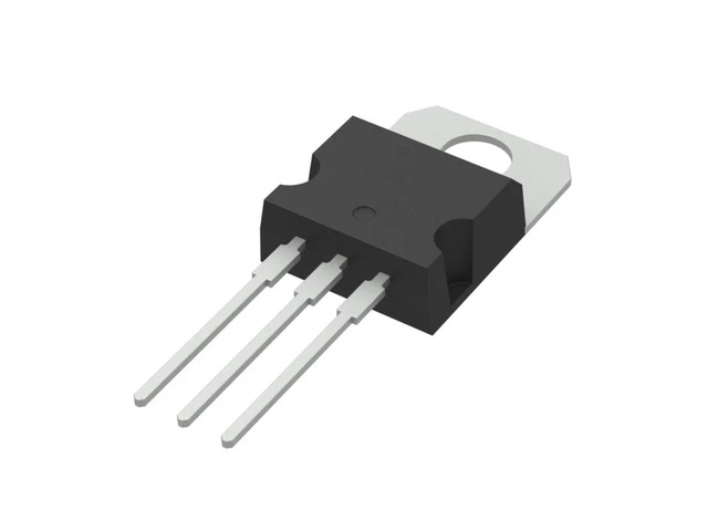
Click for zoom
STMicroelectronicsIRF 630
STMicroelectronics IRF630 N-Channel Power MOSFET 200V 9A TO-220, suitable for switching power supplies, DC-DC converters, power converters, load control circuits, industrial electronics and general switching applications.
The IRF630 by STMicroelectronics is an N-Channel STripFET Power MOSFET in a TO-220 package. It features 200V Drain-Source voltage, 9A continuous Drain current at 25°C and 0.40 Ohm max RDS(on) with 10V gate drive. The TO-220 package allows heatsink mounting for improved thermal dissipation in power applications.
Technical description
The IRF630 is a power MOSFET for switching applications, featuring low input capacitance, minimized gate charge and high dv/dt ruggedness. Pin configuration is Gate on pin 1, Drain on pin 2 and metal tab, and Source on pin 3. Proper gate drive, typically 10V, is required for full enhancement.
Typical applications
Suitable for switching power supplies, DC-DC converters, industrial control circuits, load drivers, voltage converters, power electronics, PWM circuits and general applications requiring a 200V N-Channel MOSFET in TO-220 package.
Compatibility note
The IRF630 is an N-Channel MOSFET and not an IGBT, TRIAC or thyristor. Before replacement, verify the TO-220 package, pin configuration, VDS voltage, ID current, RDS(on), gate charge and thermal requirements of the application. It is not a logic-level MOSFET, so direct drive from 3.3V or 5V microcontrollers is not recommended without a suitable driver when full enhancement is required.
Weight: approximately 0.002 kg.
Package weight: 0,002kg
Package volumetric: 0,002kg


Monday-Friday: 08:00 - 17:00
Saturday: 08:00 - 15:00
+30 210 2620250 | info@tridimas.gr
