 EL
EL EN
EN


- PC Hardware
- Wi-Fi Equipment
- Alarm Systems
- CCTV
- Satellite systems
- Terrestrial systems
- Instruments
- Plastic optical fibers
- Structured Cabling
- Telephonic
- Cabines - Racks
- Industrial Automation
- Solar panels
- FAN,Cooling Systems
- Relay
- Relay 3V
- Relay 5V
- Relay 6V
- Relay 9V
- Relay 12V
- Relay 24V
- relay 48V
- Relay 110V
- Relay 220V
- Automotive Relay
- Industrial Relay Bulb Type Base
- Relay 12VDC bulb type 8p
- Relay 12VDC bulb type 11p
- Relay 12VAC bulb type 8p
- Relay 12VAC bulb type 11p
- Relay 24VDC bulb type 8p
- Relay 24VDC bulb type 11p
- Relay 24VAC bulb type 8p
- Relay 24VAC bulb type 11p
- Relay 48VDC bulb type 8p
- Relay 48VDC bulb type 11p
- Relay 48VAC bulb type 8p
- Relay 48VAC bulb type 11p
- Relay 60VDC bulb type 8p
- Relay 60VDC bulb type 11p
- Relay 110-120VDC bulb type 8p
- Relay 110-120VDC bulb type 11p
- Relay 110-120VAC bulb type 8p
- Relay 110-120VAC bulb type 11p
- Relay 220-230VAC bulb type 8p
- Relay 220-230VAC bulb type 11p
- Relay Impulse step
- Relay on Board
- WiFi Relay
- Various Relay
- Electronic assemblies
- Electronic equipment
- Service parts
- IC
- Optocoupler
- 24LC series
- 4N series
- 5L series
- 74 series
- 78 series
- AD series
- ATT series
- CA series
- CNY series
- DS series
- F series
- H series
- ICL/ISL series
- I series
- K series
- L series
- LM series
- MAX series
- M series
- MOC series
- N series
- NJM series
- OPA series
- PC series
- PLS series
- R series
- SG series
- S series
- STK series
- STRF series
- TC series
- TDA series
- TEA series
- TL series
- TM series
- TN series
- UCxx series
- ULxx series
- V series
- Viper series
- Z series
- Logic series
- IC sockets
- TRN-MOSFET-IGBT
- IGBT-Module
- 2N series
- 2SA series
- 2SB series
- 2SC series
- 2SD series
- 2SK series
- 2SJ series
- 3N series
- 60N series
- 6NK series
- 7824 series
- 7NK series
- A series
- BC series
- BD series
- BF series
- BS series
- BU series
- BUH series
- BUZ series
- F series
- IG series
- Η series
- I series
- IP series
- IR series
- IX series
- J series
- MJ series
- N60 series
- S series
- SUD series
- T11 series
- TCM series
- TI series
- TOP series
- TS series
- ZTX series
- Accessories
- Transformers
- Relay sockets
- Switches
- Terminal blocks
- Pins
- Pins set
- Hole pin with insulation
- Spade pin with insulation
- Brass-copper female pins with insulation
- Brass-copper male pins with insulation
- Brass-copper bifurcat. with insulation
- Terminal pins with insulation
- Bullet pins female with insulation
- Bullet pins male with insulation
- Butt connectors with full insulation
- Brass female pins with full insulation
- Brass/Nylon fem. pins with full insul.
- Brass/Nylon male pins with full insul.
- Brass/Nylon fem. pins (UL) full insul.
- Brass/Nylon male pins (UL) full insul.
- Brass/Nylon/Stud flag female pins
- Midway wire connector pins
- Bridges
- Diodes
- Zeners
- Fuses
- Fuse Holders
- Fuse switches
- Thermostats
- Thermistors
- Varistors
- Thyristor - Triac
- Trimmers
- Potentiometers
- Potensiometer knobs
- Capacitors
- Pin headers
- Resisotrs
- Light resistors
- CD-DVD Laser heads
- Crystals - Resonators
- Cleaning Products
- Spray
- Chemical
- Conductive
- IC
- Batteries
- Instruments - tools
- Piergiacomi Tools
- ClampMeter
- Phase-detectors
- Multimeters
- LCR Meters
- Multimeter terminals
- Voltage testers
- Sweep function generators
- Oscilloscopes
- Temperature sensors
- Panel instruments
- Panel indicators
- Cable testers
- Soldering iron stands
- Soldering irons
- Solder for soldering irons
- Soldering Aids-Flux
- Glues
- Desoldering wicks
- Toolboxes
- Screwdrivers
- Magnetize / demagnetize tools
- Drillers
- Hobby vises
- Silicon Glue & pistols
- Hot air pistols
- Tweezers
- Rasps
- Cutting tools
- Pliers
- Wire stripping tools
- Magnifiers
- Cable stripping tools
- Wrenches/Spanners
- Coaxial connectors presses
- Cleaning brushes
- Desoldering pumps
- Soldering iron sprays
- Grounding bracelet
- Fish tapes
- Accessories set
- Antistatic gloves
- Various tools
- Consumables
- Cables
- Cabling
- A/V Converters
- Jacks - Adaptors
- RadioControl Devices
- Remote controls for All
- Connectors
- Devices
- Telephone devices
- Telephone exchange
- Digital cameras
- Audio devices
- Intercom
- Torches
- Calculators
- Clocks / thermometers / alarm clocks
- Cash testers
- Remote control testers
- Compasses
- Blood pressure monitors
- Mice persecutors / repellers
- Seasonal/hobby/gadgets
- Heaters - stoves
- Personal care
- LCD - TFT TV & Monitors
- Bags for vacuum cleaners
- Devices wall mount
- Radiocommunications
- Car accessories
- Microph. / Earphones
- Audio systems
- Professional lighting
- Power Supplies
- Alarm / CCTV
- Laboratory
- Switching power supplies in BOX
- Built in Power Supply
- Built-in Power Supplies with Buffer
- Switching Din rail
- for Laptops
- for tablets
- Mobile phone chargers
- Simple power supplies
- USB power supply
- LED power supplies
- Inverters
- Converters DC/DC Volt
- Battery chargers
- Autotransformers
- Gathering / apicultural
- Variac
- Electrical equipment
- Multiplugs
- Extension cord spools
- Cables
- AC sockets
- Floodlight-Sensors
- UPS
- Voltage stabilizers
- Outdoor watertight boxes
- Sealed boxes
- Metallic boxes
- Plastic boxes
- LED lighting
- Lamps
- Night lights
- Illuminants
- Lampholders
- Overload protection
- House equipment
- Electrical fuses
- Tubes - ducts
- Insulating tapes/spirals
- Measuring tapes
- Grommet rubbers
- Cable glants
- Cable clips / roka
Click for zoom
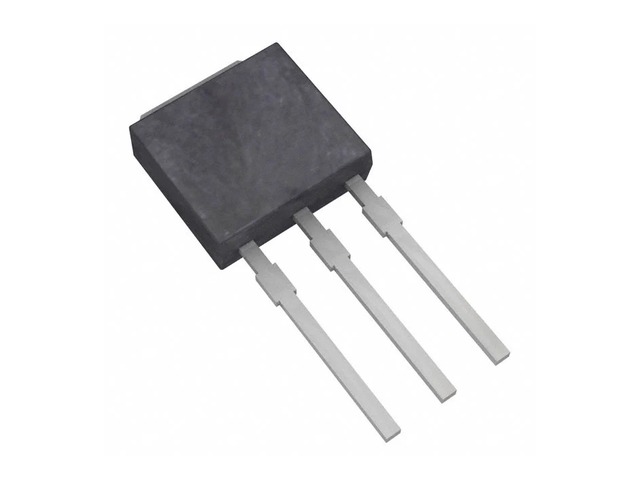
INFINEONIRFU 024N
IRFU024N N-Channel HEXFET Power MOSFET 55V 17A I-PAK / TO-251AA by International Rectifier / Infineon, suitable for power switching applications, DC loads, power supplies, PWM control, automation circuits and electronic projects.
The IRFU024N is an N-Channel HEXFET Power MOSFET from International Rectifier, now Infineon, in an I-PAK / TO-251AA straight-lead through-hole package. It features 55V maximum Drain-Source voltage, continuous Drain current up to 17A and RDS(on) of 75mOhm max at VGS 10V. It is suitable for low and medium power applications requiring fast switching and reliable operation.
Technical description
The IRFU024N is used as an electronic switch in DC circuits, power supplies, PWM drivers, small motor controllers and load switching applications. The I-PAK / TO-251AA package is a straight-lead through-hole type and is mechanically different from the IRFR024N SMD version, which uses the D-PAK / TO-252 package. For higher current applications, thermal dissipation and PCB layout must be considered.
Typical applications
Suitable for DC motor control, PWM switching, LED drivers, power supplies, load switches, battery powered circuits, automation systems, electronic projects, small power converters and general DC load switching applications.
Compatibility note
The IRFU024N is an I-PAK / TO-251AA through-hole MOSFET and is not mechanically identical to TO-220 components. It should also not be confused with the IRFR024N, which is the SMD D-PAK version. It is not a logic-level MOSFET. Low RDS(on) and full enhancement typically require approximately 10V gate drive.
Weight: approximately 0.001 kg.
Package weight: 0,001kg
Package volumetric: 0,001kg


Monday-Friday: 08:00 - 17:00
Saturday: 08:00 - 15:00
+30 210 2620250 | info@tridimas.gr
